


Current location:
According to reports, according to Ray Wang, TSMC has announced the latest progress of its advanced process roadmap, confirming that the development process of the next generation A14 (1.4nm) process is smooth, and its key yield performance has met internal expectations ahead of schedule, achieving a significant technological upgrade compared to 2nm.
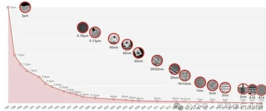
Specifically, the A14 process has achieved a comprehensive leap in performance, power consumption, and density compared to the upcoming N2 (2 nanometer) process.
The official data cited is as follows:
-Under the condition of constant power consumption, the operating speed of A14 process will be increased by 15%;
-At the same speed, power consumption can be reduced by up to 30%;
-The transistor density will also increase by 20%, allowing the chip to accommodate more functional units in a smaller space.
These significant performance improvements are attributed to the innovation of underlying technologies. TSMC revealed that the A14 process will fully adopt the second-generation GAAFET (fully surround gate) nanosheet transistor technology, combined with the new NanoFlex Pro standard cell architecture.
GAAFET technology can more effectively control current, reduce leakage, and thus control power consumption while improving performance. The new architecture further optimizes chip design, achieves higher integration, and jointly drives breakthroughs in the A14 process.
Customers such as Apple, Nvidia, AMD, etc. have planned to adopt the A14 process, and their technological empowerment of end products is worth looking forward to. TSMC expects A14 to enter mass production in 2028, further consolidating its leading advantage in advanced processes.
*Disclaimer: The above content is reproduced on the WeChat official account of the semiconductor industry circle, which does not represent the views and positions of the company, but only for exchange and learning. If you have any questions or objections, please contact us.
TVS/ESD Diode Transistor MOS FET LDO Hall IC BLCD controller